When

Thursday, December 5, 2024 - 4:00 p.m.
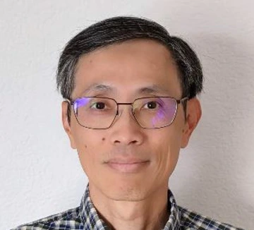
Li-Sheng Weng
Principal Architect at Qualcomm
"Chiplets Architecture and Advanced Semiconductor Packaging Integration"
AME Lecture Hall, Room S212
Zoom link

Abstract: Moore's Law has been the technical and economical driving force for process node scaling to enable higher transistor density in a monolithic system-on-chip (SoC) architecture design for decades. However, cost pressure and longer cycle time to manufacture a monolithic SOC design in recent process generations have slowed down the node scaling and forced chip designers to explore new architectures to meet higher performance generation over generation more economically. Chiplet-based architectures with high density interconnect packaging integration for homogeneous and/or heterogeneous node(s) offers a new way of designing chips to allow for more flexibility and scalability with creation of chiplets tailored to specific applications and easier to upgrade. In this seminar, we'll review the current industry landscape of 2.5D and 3D integration solutions, which enable higher off-chip interconnect density and thus higher data bandwidth, power efficiency and lower data communication latency. The broader industry trend of 2.5D/3D interconnect architecture strategy and optimization will also be highlighted in this study.
Bio: Li-Sheng Weng is a principal architect at Qualcomm. He specializes in advanced silicon package architecture definition, as well as silicon-package-system co-design. He also works on high-density interconnect and forward-looking product and technology roadmaps. Prior to joining Qualcomm, he held positions at AMD as a fellow and Google as a technologist. At AMD, he managed a team responsible for implementing package designs with optimized signal integrity, power integrity, and power delivery networks. During his time at Google, he collaborated with a team to develop a best-in-class on-device GenAI accelerator architecture that met the device's power and thermal constraints. He started his professional career with Intel, where he focused on silicon and package design integration.
Li-Sheng earned his BS degree from National Cheng Kung University in Taiwan, followed by a MS and PhD in structural engineering from UCLA. He is the holder of 32 granted and pending U.S. patents, along with multiple publications in the domains of AI accelerators, semiconductor architecture and packaging.
